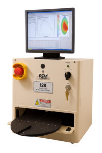
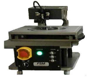
FSM 128L Film stress and wafer bow measurement for wafers up to 300mm diameter. 2D/3D stress mapping standard. Semi-automated system with convenient wafer loading.
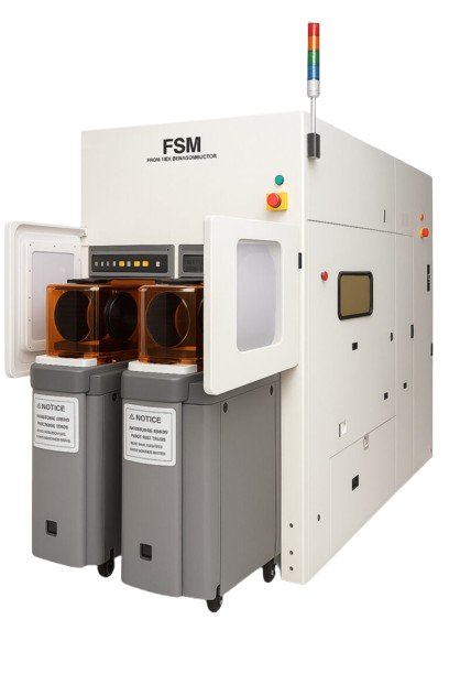
The FSM 128C2C series is a fully automated system designed for stringent production environments, including next-generation devices in 300mm fabs, III-V, and MEMS industries.
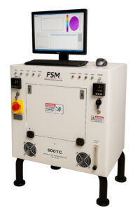
FSM 500TC Bow Height, Stress Hysteresis Measurement up to 500C for thermal property and stability tests of thin films during thermal cycling up to 500 degrees C in inert gas.
FSM 900TC Rapid Thermal Mechanical Characterization of novel materials. Simultaneous extraction of stress hysteresis, thermal desorption during thermal cycling up to 900C.
FSM413-MOT Thickness and total thickness variation (TTV) mapping system. TTV & Thickness, Roughness of wafer, thick layers, wafers on tape & bonded wafers under various conditions.
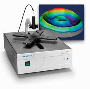
F50s are general-purpose film thickness measurement instruments, and are used in thousands of applications worldwide. Thickness measured in less than a second.
The W SERIES MICRO XRF uses poly-capillary optics to focus the X-ray beam to 7.5 µm FWHM, the world’s smallest for coating thickness analysis using XRF instruments.
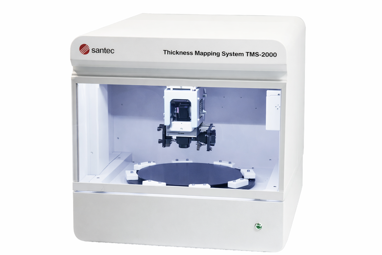
The TMS-2000 is an advanced wafer thickness and flatness measurement system designed for high precision, achieving repeatability levels as fine as 1 nanometer.
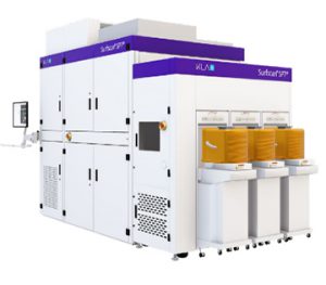
The Surfscan® SP7XP unpatterned wafer inspection system facilitates qualification and monitoring of processes and tools for IC, wafer and materials manufacturers.
W SERIES MICRO XRF uses poly-capillary optics to focus the X-ray beam to 7.5 µm FWHM, the world’s smallest for coating thickness analysis using XRF instruments.